Creating a Custom 32-bit Pipelined RISC-V SoC with a hardware accelerated Field Oriented Control (FOC) Engine.
Note that this project is in its final stages of hardware testing, but still isn’t quite finished
Introduction
For a long time I imagined CPUs as an impossibly complex technology which required teams of people to understand. When I took my Digital Systems course, however, I learned about the layers of abstraction that digital design presents, which all of a sudden made the idea of making my own CPU seem more achievable. Despite this, I learned many people had built CPUs in their own time and it was a fairly common project. To separate myself I decided to look to my other interest area, robotics/controls. This led me down quite the rabbit hole until I learned about Field Oriented Control (FOC).
BLDC motors have always been a bit mysterious to me. I first came into contact with them by accident. I was making a solar-powered cardboard car a few years back for the UBC Physics Olympics, and after some research, BLDC motors seemed so much more efficient because there’s no friction losses. So I bought one but quickly realized there was no easy way to control it via DC current, and given the weight and power constraints of the car, it frankly was not viable to have hardware to control it. So eventually we bought small DC motors and went on our merry way, but I never truly learned how to control it.
This project is then 3-fold. Teach myself computer architecture and pipelining to understand thoroughly how a CPU works, figure out how to control a BLDC motor and learn all about FOC control, and combine them together making a complete SoC synthesized on an FPGA that drives the motor. Although this was a daunting task, I gave myself most of my summer free time to figure it out.
For a complete set of features and specs, check out my GitHub repo for the project here.
CPU Design
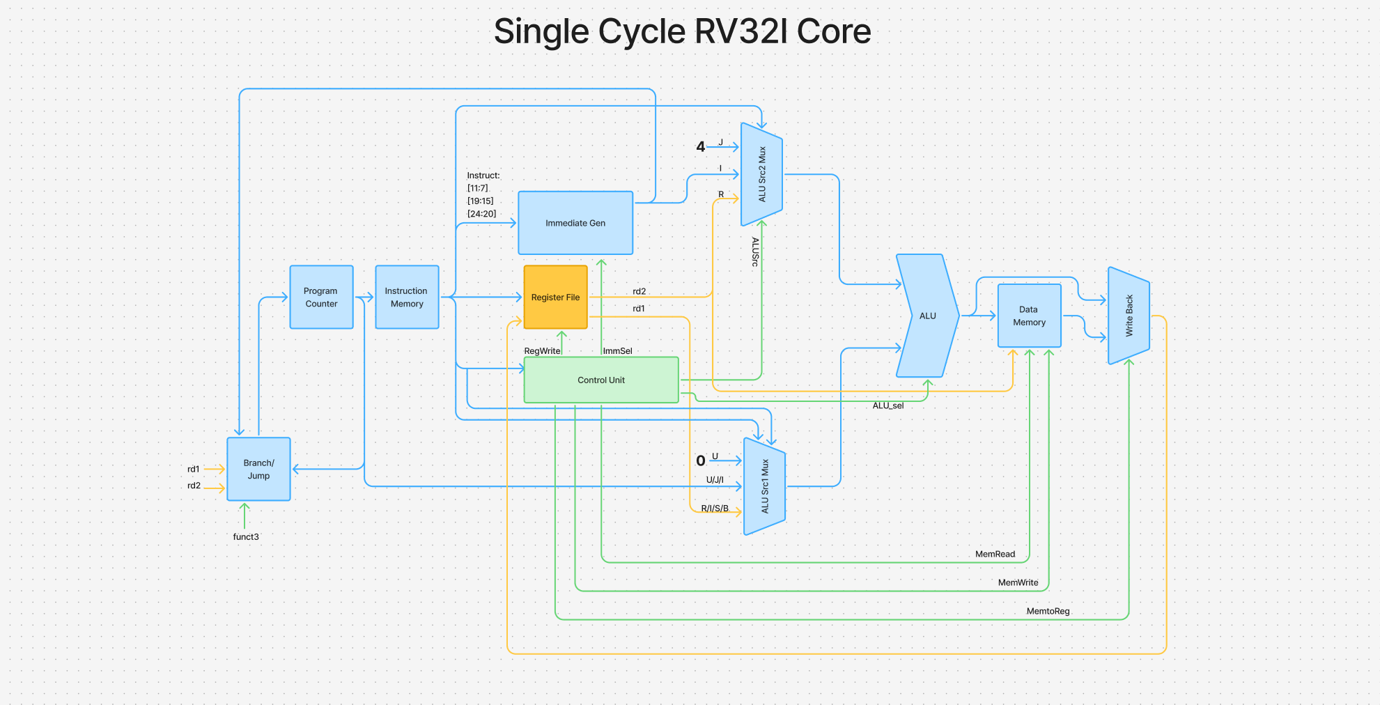
Single Cycle CPU
First things first, before I could do anything fancy I figured a simple RISC-V core with no bells and whistles would be a good starting point. I decided on a 32-bit architecture since the added precision would likely be nice for the FOC and there were lots of helpful resources. Although all modules were completely written by me, the official RISC-V documentation, along with the Digital Design and Computer Architecture textbook by Harris and Harris were super useful throughout.
Since the single cycle CPU isn’t too interesting, I figured I would talk about my process and main challenges I found.
I broke the processor down into modular blocks:
- Datapath: Program Counter (PC), Instruction Memory, Register File (32 x 32-bit registers with hardwired
x0 = 0), Immediate Generator (ImmGen), and the ALU. - Control Unit: Main Decoder (generating control signals from
opcode) and ALU Decoder (refining ALU operations usingfunct3andfunct7).Hardware Nuances & Traps
A few subtle digital design quirks showed up during the single-cycle bring-up:
- Read-During-Write Register File Hazard: If an instruction writes to a destination register while the next module attempts to read the same register in the same clock cycle, reading the register array directly yields stale data. I solved this by adding an internal combinational bypass in the register file: if the write enable is high and write address matches read address, it forwards the input data immediately.
- Strict 4-State Verification (
===vs==): In SystemVerilog, standard equality (==) can mask uninitialized ('X') or floating ('Z') values. Switching to case equality (===) in unit testbenches ensured that undriven buses were caught immediately. - Testbench Independence: I quickly learned an important rule of hardware verification: never mirror your module’s internal logic inside the testbench. Doing so creates a false sense of security where bugs in logic simply validate bugs in tests.
Once I was all done though, I synthesized the top module and ran it on my DE23-lite FPGA. I wired the switches on the FPGA directly to the ALU to act as a calculator, and wired a button to rst_n. After some finicking with Quartus, it worked well and thus it was time to move on to a more complex design.
Single Cycle CPU Diagram
5-Stage Pipelined CPU
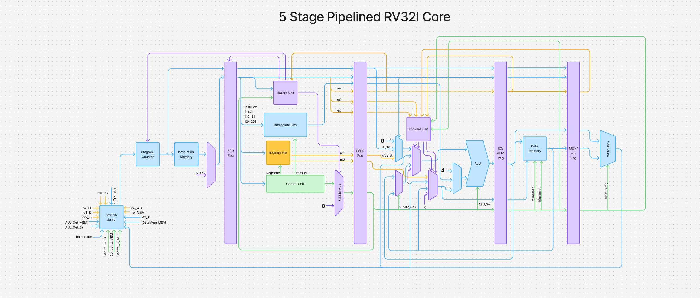
Implementing a 5-stage pipeline would allow me to both improve performance of the CPU substantially, while also gaining a deeper understanding of computer architecture. As for why I chose 5 stages over say 7 or 3, it seemed like a good balance between complexity and performance which wouldn’t be too daunting for my first pipeline.
For an overview of the architecture, it was again, fairly standard, and based on a diagram from the textbook I was reading. But to break it down:
- IF (Instruction Fetch): Read instruction from Imem and update PC.
- ID (Instruction Decode): Decode opcode, read register file, and sign-extend immediates.
- EX (Execute): Perform ALU operations or calculate memory/branch addresses.
- MEM (Memory Access): Read or write data to DMem.
- WB (Writeback): Commit the final result back into the register file. I inserted pipeline registers (
IF/ID,ID/EX,EX/MEM,MEM/WB) to isolate each stage. However, slicing the datapath immediately introduced the hardest challenge in processor design: Hazards.
The Hazard & Forwarding Unit: Solving Pipeline Bottlenecks
Without hazard handling, instructions in flight would compute with stale register values or execute invalid instructions after a branch.
I designed a dedicated Hazard Unit to manage data dependencies and control flow:
Data Forwarding (Bypassing)
Normally, an instruction doesn’t write its result to the register file until the WB stage. If a consecutive instruction needs that value in EX, it would normally have to stall for 2 cycles. I implemented forwarding muxes that route the result directly from the EX/MEM or MEM/WB pipeline registers back into the ALU inputs as soon as it’s computed.
The Load-Use Hazard (Why lw Needs a Stall)
Forwarding solves most data hazards, but there is a physical limitation with memory loads (lw). The loaded data isn’t valid until the end of the MEM stage. If the very next instruction needs that loaded value in EX, it is traveling backward in time. To fix this, the Hazard Unit detects if the instruction in EX is a load and its destination matches an operand in ID. If so, it:
- Freezes the PC and
IF/IDregister for 1 cycle. - Injects a bubble (NOP) into the
ID/EXregister (clearing control signals). Forwards the loaded memory data on the following cycle from
MEMtoEX.Automated Verification: Python CRT & Differential Fuzzing
Debugging a pipelined processor with hand-crafted testbenches is nearly impossible because multi-instruction hazard bugs only occur under specific sequences of dependencies and branch conditions. To thoroughly verify the core, I created an automated Differential Testing / Co-Simulation harness:
- Constrained Random Testing (CRT): I wrote a Python generator that produced random, valid RV32I instruction streams.
- Differential Comparison: I simulated the machine code in SystemVerilog while simultaneously running the exact same binary on a verified golden reference simulator.
- Register/Memory State Dumps: The harness compared the register state instruction-by-instruction.
The Bugs It Exposed:
- Initial 80% Failure Rate: Early random CRT runs failed 8–9 times out of 10. Tracing instruction-by-instruction revealed a read-during-write hazard where an instruction in
WBwas writing to a register at the exact moment another instruction inIDwas reading it. Adding a combinational forwarding bypass inside the register file resolved this. - Scaling to 20,000 Instructions: After fixing basic forwarding, short tests passed. But when I scaled the fuzzer to stress-test runs of 20,000 instructions, new edge cases emerged:
- PC Enable Bug: During load-use stalls, the PC was still updating because the stall enable condition wasn’t properly gating the PC register.
- Load-Forwarding Race: A bug in the forwarding priority logic was attempting to forward an unread memory value to the ALU before the
MEMstage had actually latched the data. Once the pipelined core could execute 20,000+ random instruction fuzzing runs with 100% state matching against Venus, the RISC-V processor was rock solid and ready to host the FOC accelerator.
After fixing the bugs, and finding that the CPU had a 1.12 CPI from the CRT I made, I created a Quartus file to find fmax of the processor on my DE23-lite. The fmax of the 5-stage pipelined core was 192.42 MHz. Although this is good, when I checked the single cycle, it was at 138.45 MHz. Using the speedup equation below, the speed increase from pipelining is shown.
Using the fundamental processor performance equation ($\text{Time} = \frac{\text{Instructions} \times \text{CPI}}{f}$), the overall speedup from pipelining is:
\[\text{Speedup} = \frac{\text{Execution Time}_{\text{single}}}{\text{Execution Time}_{\text{pipelined}}} = \frac{\text{CPI}_{\text{single}} \times F_{\text{max, pipe}}}{\text{CPI}_{\text{pipe}} \times F_{\text{max, single}}}\]Plugging in my measured numbers:
\[\text{Speedup} = \frac{1.0 \times 192.42\text{ MHz}}{1.12 \times 138.45\text{ MHz}} = \frac{192.42}{155.064} \approx 1.241\times\]Or evaluated by effective throughput:
- Single-Cycle: $\frac{138.45\text{ MHz}}{1.0\text{ CPI}} = 138.45\text{ MIPS}$
- 5-Stage Pipelined: $\frac{192.42\text{ MHz}}{1.12\text{ CPI}} = 171.80\text{ MIPS}$
This represents a $+24.1\%$ real-world throughput improvement. Despite this, I understand that although improved, this speedup is not nearly as close to the theoretical 5x speedup, or even the realistic 3x speedup. Although I have not figured out the exact reason that is yet, I have theorized that because of the faster FPGA architecture, maybe most processes are sped up in general, but there could be one element that’s majorly bottlenecking the single cycle CPU which could be the same thing bottlenecking the pipelined CPU, and that being the main reason that the speedup is not what I expected.
5-Stage Pipelined CPU Diagram
FOC Design
The last pillar of this project was to create the FOC accelerator. FOC consists of 5 main parts. The CORDIC transform to get sine and cosine, a Park and Clarke transform, a PI loop, an inverse Park and Clarke, and a PWM output. I decided to make a hybrid firmware/hardware accelerator for this so the CPU is involved in the loop, while still getting help to maintain a frequency >20 kHz to quietly control the motor.
Hardware-Accelerated & Peripherals
16-Stage Pipelined CORDIC Engine
Computing trigonometric functions ($\sin$ and $\cos$) in software on an RV32I core without a hardware multiplier (M extension) takes hundreds of cycles using Taylor series or large lookup tables (LUTs). A CORDIC (Coordinate Rotation Digital Computer) algorithm is ideal for FOC because it computes high-precision trigonometry using only bit-shifts and additions. I implemented a 16-stage fully pipelined CORDIC engine in SystemVerilog with quadrant folding, outputting full Q16.16 fixed-point sine and cosine values on every clock cycle (after a 16 clock delay).
3-Phase Center-Aligned PWM with Dead-Time Protection
The PWM controller drives the 3-phase MOSFET inverter gate driver. Hardware acceleration was necessary here to guarantee rock-solid switching timing immune to CPU stalls or pipeline bubbles. The module generates center-aligned PWM waveforms to minimize harmonic current distortion, and includes configurable hardware dead-time insertion between the high-side and low-side complementary gate outputs to prevent shoot-through (and save the inverter from a magic-smoke incident).
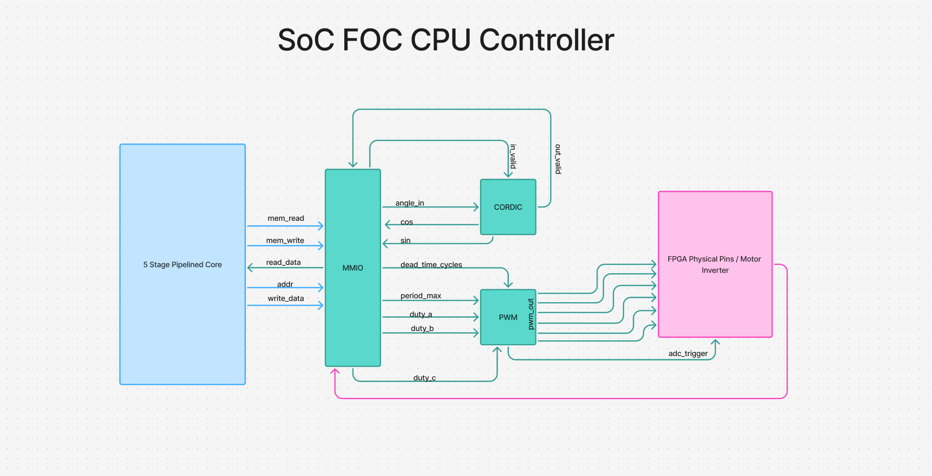
Custom Memory-Mapped I/O (MMIO) Bus
To allow the C firmware to communicate with the accelerators, I built an MMIO address decoder (foc_MMIO.sv) that routes accesses above 0x8000_0000 to internal registers. The CPU configures PWM dead times and period counters, feeds electrical angles to the CORDIC, and writes DUTY_A/B/C compare thresholds using simple sw instructions.
Autonomous High-Speed (3.33 MHz) I2C Master
Reading analog feedback via software bit-banging would overwhelm the CPU. I wrote a dedicated 3.33 MHz High-Speed I2C master in SystemVerilog to stream data from the on-board TI TLA2528 12-bit SAR ADC. I wrote this because the on-board ADC on the DE23-lite uses this chip to read the voltage. Although I2C isn’t ideal for fast communication, typically at 400 kHz, at the 20 kHz FOC I want to use, the period would be 50 µs. Since I need to transmit 64 bits over I2C, that would take around 21 µs at 3.33 MHz, which then can compute within the period meaning it would work. This was made by using an FSM which turns on the chip at 400 kHz sets it to High-Speed mode and then reads the constant stream of data.
Firmware Accelerated
While the time-critical trigonometry, PWM generation, and I2C serialization were offloaded to hardware, the core vector math and closed-loop control algorithms were implemented in bare-metal C running on the RV32I core. This hybrid approach allows the CPU to dynamically tune PI gains and control parameters in software while easily keeping up with the fast loop execution.
Vector Space Transforms (Clarke & Park in Q16.16)
The firmware executes forward vector transforms to project measured 3-phase currents into the rotor’s rotating reference frame. The Clarke transform first converts 3-phase currents into stationary orthogonal 2-axis coordinates ($I_\alpha, I_\beta$) using fixed-point multiplication with $1/\sqrt{3}$ (ONE_BY_SQRT3_Q16 = 37838). The Park transform then rotates these coordinates into the rotor-aligned $d-q$ frame ($I_d, I_q$) using the sine and cosine values read directly from the CORDIC hardware accelerator.
Dual Discrete-Time PI Current Regulators
Current regulation is performed using two independent, discrete-time PI controllers operating in the rotating $d-q$ frame. The direct-axis ($d$-axis) target is set to $I_d^* = 0$ to ensure all current produces torque rather than wasted magnetic flux. The quadrature-axis ($q$-axis) target ($I_q^*$) acts as the active torque command. Both controllers include proportional and integral accumulation with strict clamping limits (VMAX) to prevent integrator windup during rapid load or setpoint changes. To tune the gains, I used a simple python script using the bandwidth frequency and associated equations to calculate Kp and Ki.
Inverse Transformations & PWM Duty Scaling
Once the PI controllers output target voltage vectors ($V_d, V_q$), the firmware converts them back into phase commands. The Inverse Park transform rotates $(V_d, V_q)$ back into the stationary frame $(V_\alpha, V_\beta)$ using CORDIC $\sin/\cos$. The Inverse Clarke transform then decomposes these orthogonal vectors into 3-phase sinusoidal voltages ($V_a, V_b, V_c$). Finally, a scaling function offsets each voltage to the center of the PWM counter period (half_N), clamps the bounds, and writes the updated compare thresholds directly to the DUTY_A/B/C MMIO registers.
Real-Time Hardware/Software Synchronization
The entire FOC loop runs deterministically synchronized to the hardware PWM frequency. The CPU polls FOC_STATUS_REG until the hardware finishes streaming feedback data at the center of the PWM cycle. Once triggered, the core fetches data, computes the forward transforms, updates the PI loops, applies the inverse transforms, pushes new duty cycles to the PWM registers, and clears the status register to wait for the next switching period.
Full SoC
By connecting the peripherals to the CPU and FOC, and making DataMem available to both, I formed the full SoC which can be shown in the diagram below.
Synthesizing the Full SoC
Now that the full SoC is put together, the final step is running it on real hardware. This is obviously the most important but also complex as Murphy’s Law states that everything is going to go wrong, so we will see.
Hardware used
Terasic DE23-Lite FPGA Development Board
The design is targeted to the DE23-Lite board. The board provides an on-board 50 MHz clock source, plenty of logic elements and block RAM for the SoC, and an integrated TI TLA2528 8-channel 12-bit SAR ADC. The FPGA communicates with the ADC chip internally over I2C (PIN_M2 for SCL, PIN_N2 for SDA), while the analog input channels are broken out on the 2x5 header (J4) for direct sensor wiring.
2804 Brushless Gimbal Motor
I selected a 2804-size BLDC gimbal motor for the physical demonstration. Gimbal motors feature a high-pole 12N14P construction (7 electrical pole pairs per mechanical revolution) and a high phase resistance ($R \approx 5\text{–}15\,\Omega$). This high winding resistance limits peak currents to safe levels ($< 1.0\text{ A}$ at 12V), making it ideal for tabletop development without risking thermal runaway or damaging the power stage.
AS5600 Magnetic Rotary Position Sensor
To provide high-resolution rotor angle feedback for the Park and Clarke transforms, I mounted an AS5600 12-bit magnetic rotary encoder directly over a diametrically magnetized magnet attached to the motor shaft. The sensor is configured in its 3.3V analog output mode, producing a linear $0\text{V} \rightarrow 3.3\text{V}$ voltage proportional to the $0^\circ \rightarrow 360^\circ$ mechanical angle. This signal is fed into ADC channel 7 (ADC_IN7), giving approximately $0\text{ to }2703$ counts across a full rotation.
Allegro ACS712 Current Sensors
Phase currents $I_a$ and $I_b$ are measured using isolated Hall-effect current sensor modules based on the Allegro ACS712. Powered from the 5V rail on header J4, the sensors produce a voltage centered at $V_{CC}/2 = 2.5\text{V}$ at zero current. As current flows bidirectionally through the motor windings, the output swings between $0.5\text{V}$ and $4.5\text{V}$, which maps cleanly into ADC channels 4 and 5 (ADC_IN4 and ADC_IN5) without requiring external level-shifting circuitry.
3-Phase Inverter & Gate Driver
A 3-phase MOSFET bridge inverter handles power delivery to the motor coils. The inverter receives 6 complementary logic signals (pwm_ah, pwm_al, pwm_bh, pwm_bl, pwm_ch, pwm_cl) routed through the DE23-Lite’s 40-pin GPIO header (JP1). The hardware dead-time generator in the SoC guarantees that high-side and low-side FETs on the same half-bridge never conduct simultaneously.
Analog Throttle Potentiometer
A 10k potentiometer wired across the 5V supply and ground provides the real-time speed/torque command. The wiper voltage is connected to ADC channel 6 (ADC_IN6), allowing manual adjustment of the target quadrature current ($I_q^*$) during motor operation.
Actually Running It
This is currently in progress.