Creating a Maximum Power Point Tracking (MPPT) System For Max Charge Efficiency on Satellite
Introduction
Note on Design Iterations: The first half of this post documents the initial conceptual prototype designed in January 2026. For the flight-ready overhaul and lessons learned, see the August 2026 Architecture Update below.
As the Electrical Power Systems lead on the satellite branch of the Queen’s Space Engineering Team, I am always looking for ways to enhance all aspects of the power distribution for the satellite. One of the most vital metrics on a CubeSat is efficiency; energy is not an abundant source for them, so efficiently receiving as much power as possible is vital to have a functioning satellite. Due to this, I was looking into ways to improve efficiency, which is how I found out about Maximum Power Point Tracking (MPPT). This technology is used on variable power sources, such as solar panels, to vary apparent impedance at the source and always output the max power regardless of light intensity.
Process
Starting off, it is important to get a high-level overview of how the MPPT will function. At a high level, an MPPT is a DC-DC converter with a duty cycle that varies with the variable source to ensure max power at the current state. So my first draft was essentially this in its most bare-bones state: the solar panels attached to a DC-DC converter of some sort, connecting to a battery, then a buck converter goes from the solar array to a STM32, which then powers the duty cycle of the MPPT.
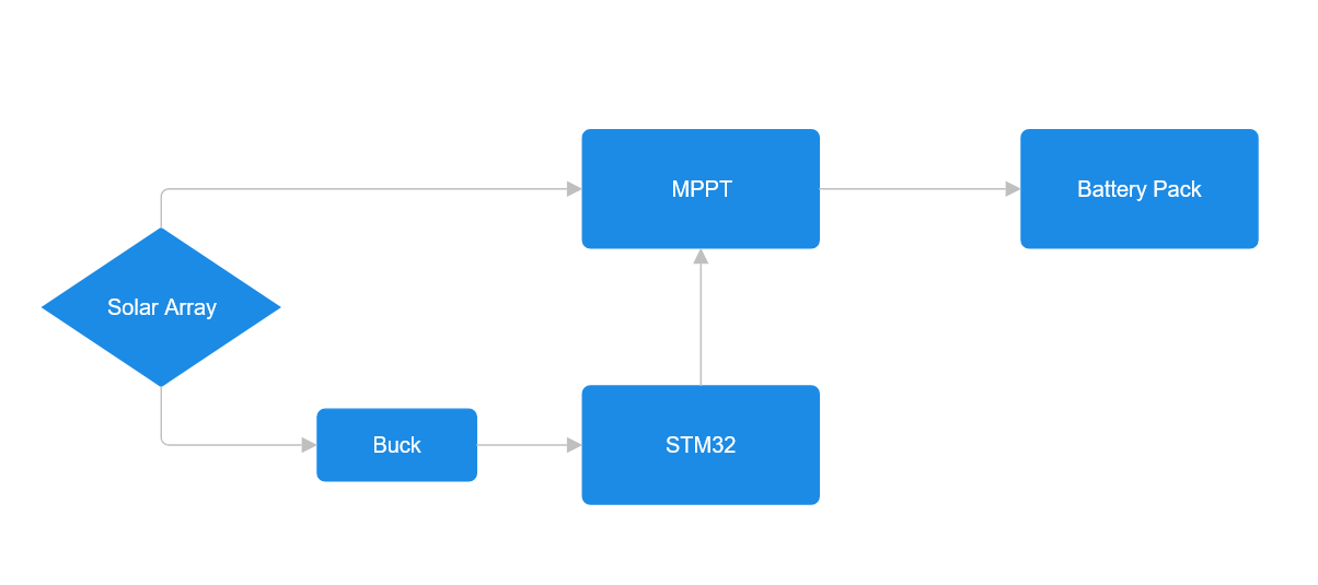
Although this is a good starting point, there are several problems that need to be addressed before moving forward with the design phase of this project. First of all, it would be less reliable to get energy to the STM from the solar panels as there can be times where minimal energy is received. Due to this, it would be smart to power the STM on a stable source like a battery. However, that presents a new problem: what happens when the batteries are dead? How does the STM start up to get the MPPT to start charging the batteries to power the STM? Additionally, there would need to be a way to power the MOSFETs on the MPPT as the STM runs on 3.3V.
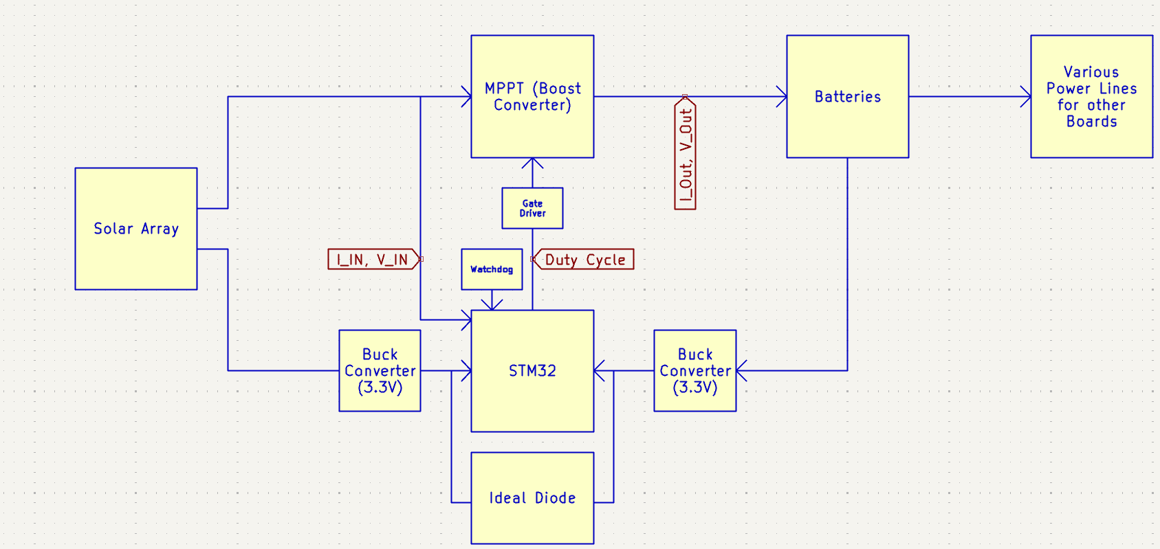
So for my next design I made the following changes: I had a buck converter which received power from batteries and solar panels, and an Ideal Diode which would compare and essentially check if the batteries were dead to see what to power the STM32 with. Then there would be a watchdog ensuring space radiation does not cause problems with the STM32, and if it does, it can be reset. Then a gate driver would run from the STM to the MPPT to ensure it can power the MOSFETs.
Below is the diagram used in KiCad to guide the design.
Design
Now that the general overview of the project has been outlined, the design process should begin. To start, getting the voltage of the solar array and battery is important. Although not finalized, I can make a safe assumption that 24 AZUR Space Triple Junction solar panels will be on the satellite along with 8 Lithium-Ion Batteries. After some consideration, I found that I should organize the solar panels in a 3s8p (series parallel) orientation allowing for a VOC of 8.1V and ISC of about 4A, and the batteries in a 2s4p orientation allowing for a max charge voltage of 8.4V. I chose these to be close to each other as a DC-DC converter is most efficient for smaller boosts. Additionally, the 8.4V is a good middle ground between 3.3V and 12V, which would allow for fairly efficient conversions to other logic levels.
Now that this is decided, and it is confirmed that the solar array will never get above the 8.4V max charge of the battery, the MPPT can be chosen to be a boost converter, which can only raise voltage. Although a buck-boost would add versatility in the MPPT, the extra space it takes up is likely not worth it for the gains.
The following is a completed table of the specs of the MPPT:
| Parameter | Value |
|---|---|
| V_in max | 8.1 V |
| I_in max | 4.16 A |
| V_out min | 5.0 V |
| V_out max | 8.4 V |
| I_out max | 5.4 A |
| P_out (max) | 26 W |
Simulation
Now that all of these specs have been selected, it is advantageous to run a simulation for the proof of concept. To do this, I used the standard boost converter equations for inductance and capacitance. Note: a freq of 200 kHz was assumed as that is a typical frequency for MPPTs controlled by STM32s.
The selection of the Inductor ($L$) and Capacitor ($C$) is not arbitrary; it is driven by the need to maintain Continuous Conduction Mode (CCM) and to meet specific signal integrity targets.
1. Determining Minimum Inductance ($L_{min}$)
The primary goal for the inductor is to prevent the current from dropping to zero during the switching cycle. This boundary is known as the Critical Inductance.
The Design Constraint: To stay in CCM, the inductor must be larger than:
\[L_{min} = \frac{V_{in} \cdot D}{2 \cdot I_{out} \cdot f_s} \cdot (1-D)^2\]Calculation for this Project: Using our parameters ($V_{in}=8.1V$, $D=0.0357$, $I_{out}=5.4A$, $f_s=200kHz$):
\[L_{min} = \frac{8.1 \cdot 0.0357}{2 \cdot 5.4 \cdot 200,000} \cdot (1-0.0357)^2 \approx \mathbf{0.12 \mu H}\]Decision Logic: While the mathematical minimum to function is only $0.12 \mu H$, a value of $33 \mu H$ was chosen. This provides a massive safety buffer, ensuring the converter stays in CCM even if the load current drops significantly (to roughly $20mA$), which prevents the unpredictable voltage spikes associated with Discontinuous Mode (DCM).
2. Determining Required Capacitance ($C$)
The output capacitor is decided by the maximum allowable “dip” in voltage while the switch is closed and the inductor is disconnecting from the load.
The Design Constraint: The required capacitance is a function of the desired voltage ripple ($\Delta V_{out}$):
\[C = \frac{I_{out} \cdot D}{f_s \cdot \Delta V_{out}}\]Calculation for this Project: If we set a strict target for high-performance signal integrity such as a 10mV maximum ripple we can solve for the required $C$:
\[C = \frac{5.4 \cdot 0.0357}{200,000 \cdot 0.010} \approx \mathbf{96.3 \mu F}\]Decision Logic: A standard $100 \mu F$ value was selected. This choice directly satisfies the $10mV$ ripple target while allowing for “Capacitance Derating” (the fact that ceramic capacitors lose some effective capacitance when operating at their rated DC voltage).
Summary of Selection Criteria
| Component | Governing Constraint | Threshold | Chosen Value | Engineering Rationale |
|---|---|---|---|---|
| Inductor | CCM Boundary | > 0.12 µH | 33 µH | Stability at light loads. |
| Capacitor | 10mV Ripple Target | > 96 µF | 100 µF | Signal integrity & DC derating. |
LTSpice Sim
By putting all of these values into LTSpice, and deciding on a synchronous boost converter for the extra efficiency gains compared to using a diode, the following plots were made, thus validating choices made. This was done at a min and max voltage with different duty cycles to ensure the voltage could stay the same.
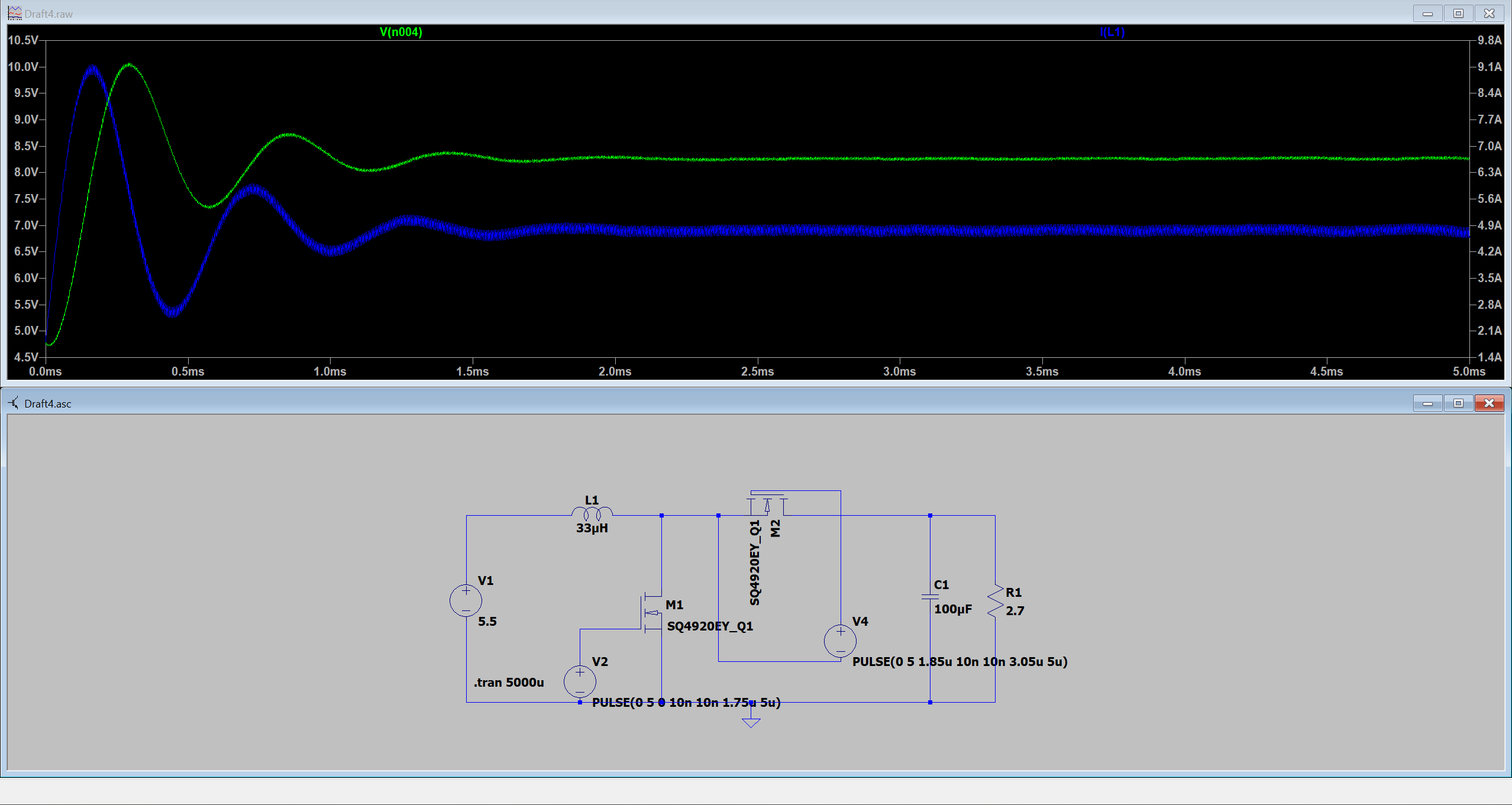
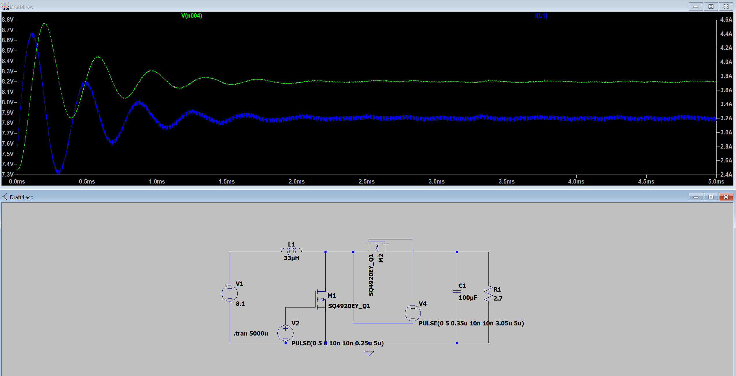
After this success, starting the design for the PCB schematic was the next step.
Schematic
Watchdog
Although separate from what I was previously testing, I decided to start the Schematic with the watchdog. For this, I decided to use a finite state machine which was controlled by D Flip-Flops and a 555 timer clock. The idea behind this was ensuring that this is purely deterministic and hardware-based means there is a lower likelihood of it failing in space. Additionally, it is made out of radiation-hardened components. Below is the design process I used, along with the schematic I made for it in KiCad.
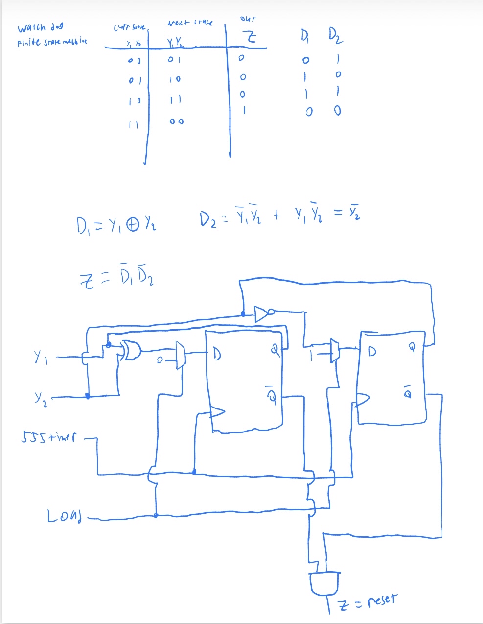
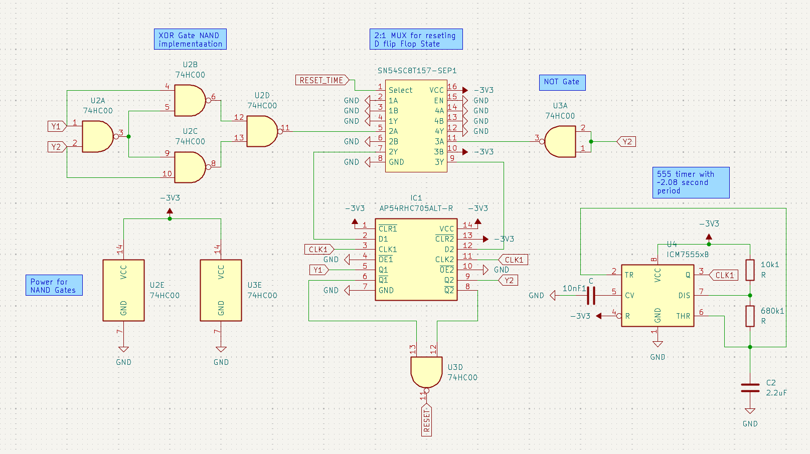
Note: I am aware of a mistake I made where the voltages are -3V3 instead of 3V3, this is fixed later on.
MPPT
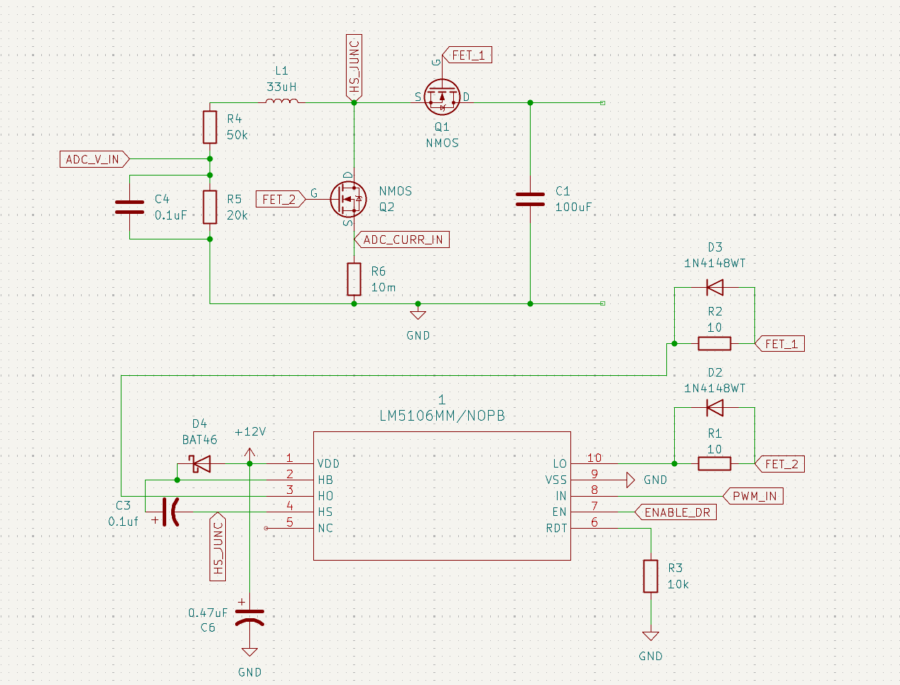
Now for the MPPT, most of the work for this had been done previously, so I mostly just needed to find a gate driver which could drive the MOSFETs and then it was smooth sailing from there. However, I did add voltage sensors using voltage dividers and Current sensors using Shunt resistors.
3.3V Logic
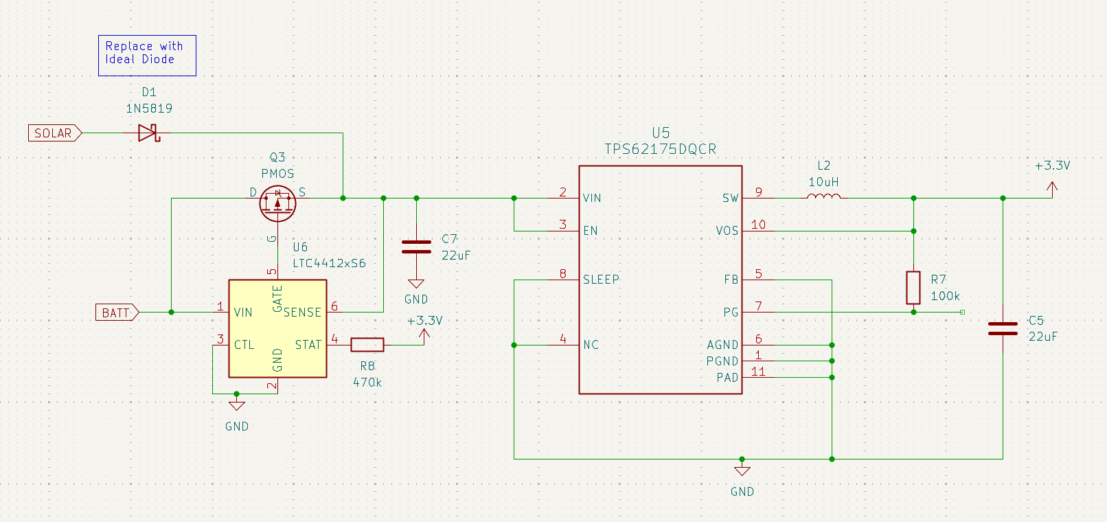
For powering the STM32, I used a buck converter IC which is capable of keeping a 3.3V output with a large variation of input voltages, and I used an ideal diode to separate the battery and solar panel but still allow for one to go through regardless of the situation the battery ends up in.
STM32
For the STM32, I ended up choosing between the L4 series for its low power and G4 series for its HRTIM which would increase the resolution of the PWM.
| Feature | STM32L4 | STM32G4 |
|---|---|---|
| Current Consumption | 100 µA/MHz | 160 µA/MHz |
| Active Current | 8 mA (80 MHz) | 27 mA (170 MHz) |
| Wattage (3.3V) | 26 mW | 89 mW |
| Precision (@ 200kHz) | 200 Steps | 13,586 Steps |
Due to the incredible extra Precision of the G4, it would get a lot closer to the true max power point, which means that a near 30W output should offset the extra power consumed. To prove this, the following shows the calculations that justify this:
Duty Cycle Resolution Calculation
The resolution is the smallest possible increment in the duty cycle ($D$), calculated as:
\[\text{Resolution} = \frac{1}{\text{Total Steps}} \times 100\%\]STM32L4 (Standard Timer):
\[\text{Res}_{L4} = \frac{1}{200} = 0.005 = \mathbf{0.5\%}\]STM32G4 (High-Resolution Timer):
\[\text{Res}_{G4} = \frac{1}{13,586} \approx 0.0000736 = \mathbf{0.00736\%}\]Comparative Analysis
| Metric | STM32L4 | STM32G4 | Difference/Factor |
|---|---|---|---|
| Control Steps (@ 200kHz) | 200 | 13,586 | 67.93x More Steps |
| Duty Cycle Step Size | 0.5% | 0.0074% | 67.93x Finer Control |
The 67.93x resolution difference fundamentally changes the performance of the Boost Converter:
- Reduced “Hunting” Loss: With the STM32L4, a $0.5\%$ step is often too “coarse.” If the ideal peak power is at a $3.75\%$ duty cycle, the L4 must oscillate between $3.5\%$ and $4.0\%$, creating a “steady-state ripple” that wastes energy.
- True Peak Tracking: The STM32G4 can move in increments of $0.0074\%$. This allows the control loop to “lock” onto the exact peak power point with virtually zero oscillation.
- Conclusion: The trade-off of using an extra $63\text{ mW}$ of MCU power (STM32G4) is justified because the precision gains allow the converter to harvest significantly more power from the solar panel often increasing total system efficiency by several percentage points compared to low-resolution control.
Big Changes (Aug 2026 Update and Finalized Design Decisions)
I wrote the first part of this report near the start of the design, since then, I’ve continued designing slowly but surely, and almost all major components from the original design have been changed, swapped out, or refined. I would like to go through in depth my design trade-offs, what motivated these changes, and the current state of the board.
Requirements
I decided if I want to properly design this without making the mistakes of the first time, I needed proper design requirements. So I went through all of the core functionalities these boards needed and created a document to store them. If you would like to see them, you can access them here:
Requirements Matrix (Google Sheets)
MPPT Changes
The MPPT is the heart of this PCB, and is one of the most pivotal circuits in the entire CubeSat. In my first iteration, this was an MCU-controlled gate driver which drove a manually made buck converter. When researching into this, I discovered many flaws with this design, however:
- Radiation Constraints: Firstly, on a student budget a radiation tolerant MCU is almost certainly unreachable. Making the entire MPPT based on the hope that the non-radhard MCU would work was silly, even for a short mission in LEO.
- Silicon Efficiency & Hot Loops: Secondly, having never worked with DC-DC converters prior, I was a bit naive about a few facts about them. Most obviously, an IC made by a company with resources and billions of dollars is almost always going to be more efficient than what I can make with discrete components. Not even considering that it would be harder to make the hot loop small, and less likely to work.
Due to this, the decision to switch to an IC buck was clear.
Another key decision made was informed by a few papers I looked at:
- Thomas S. Wurster, Markus B. Schubert (2014). Mismatch loss in photovoltaic systems, Solar Energy, Vol. 105, pp. 505–511. DOI: 10.1016/j.solener.2014.04.014
- Mohd Zulkifli Ramli, Zainal Salam (2019). Performance evaluation of dc power optimizer (DCPO) for photovoltaic (PV) system during partial shading, Renewable Energy, Vol. 139, pp. 1336–1354. DOI: 10.1016/j.renene.2019.02.072
These papers shed light (pun intended) on single vs distributed MPPT architectures. The key insight is that if two panels are in parallel and one is shaded, the effective shared max power point between them gives less power than the max power of each panel individually. Because every milliwatt matters on a CubeSat, having an MPPT for each panel could help with some extra recovery. Additionally, the CubeSat’s solar design relies on 1 panel on each side of the satellite meaning at all times at least 2 panels are shaded. Therefore, a distributed architecture was chosen for this design.
Another adjacently related flaw with an earlier assumption is the need for a boost converter. Although I had good initial justification, that the solar panels would be wired to a voltage which is always below the battery meaning no matter the sun intensity they could have energy harvested. With more research I found it was much more simple to wire all solar panels in series on 1 board meaning it would be about 16-17V. This would require a buck or buck-boost converter, adding to the reasons to change the architecture.
With a list of requirements and a solid understanding of the system’s level view of the satellite there were a few options I could go with:
- The first one would be an integrated MPPT and buck converter chip which handles most things autonomously but has some weak points when it comes to radiation.
- Alternatively, a separate chip could control the buck and MPPT, but this would add more points of failure.
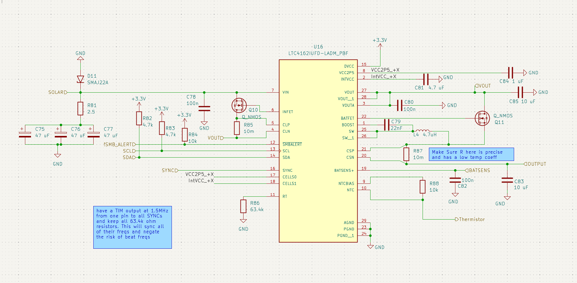
I eventually found an IC which although was not radiation tolerant, included a lot in the package making it appealing considering the minimal space on the board. This IC is the LTC4162, an integrated synchronous buck converter and MPPT controller. It is very configurable, and allows for lots of telemetry. In fact it acts as a full power-path controller allowing it to automatically account for Constant Voltage and Constant Current charging which makes life on the software side easier.
Below is the schematic used for all 4 ICs on the board (1 per panel). For some notes about the decisions made here, there are a few important things to talk about:
- Cell Configuration: First off, wiring
CELLS0toVCC2P5andCELLS1toINTVCCis the configuration used for 2 series Li-Ions which is required for this design. - Frequency & Synchronization: Another important thing, the
RTandSyncpins were chosen carefully. These allow you to configure the frequency the Buck operates at; I am tying all four to a PWM pin on the MCU to keep them all at 1.5MHz and avoid beat frequencies. As forRT, it is recommended by the manufacturer to keep it to a similar frequency, so by setting R86 to 63.4k I set it to around 1.5MHz as well in case the MCU fails.
Since these chips are not designed to work in parallel, I needed to do a few things:
- First I asked on Analog’s forums and they reassured me that it would likely be fine.
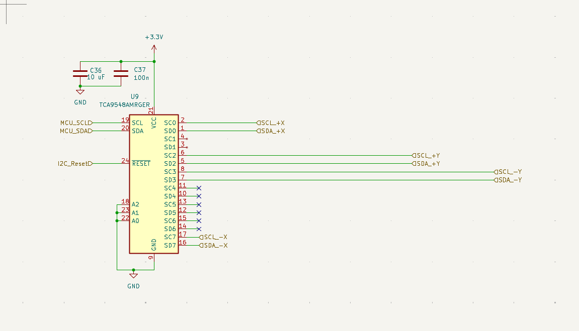
- Then since there is no reconfigurable I2C, I needed to use an I2C MUX to allow for the MCU to select which chip it is talking to. Below is the schematic for the MUX.
Watchdog Changes
In the original design, I used a (in my opinion) clever and robust FSM comprised of Rad-Hard D-Flip-Flops. Although I believe this could have worked, there are some problems I started to foresee:
- Firstly, the more components on a board the more points of failure, the more space taken, the harder routing is, and likely less efficient too.
Due to this, I looked for an IC watchdog which would do the same job and ended up finding the TPS3823A which fit my needs well. Below is the schematic used.
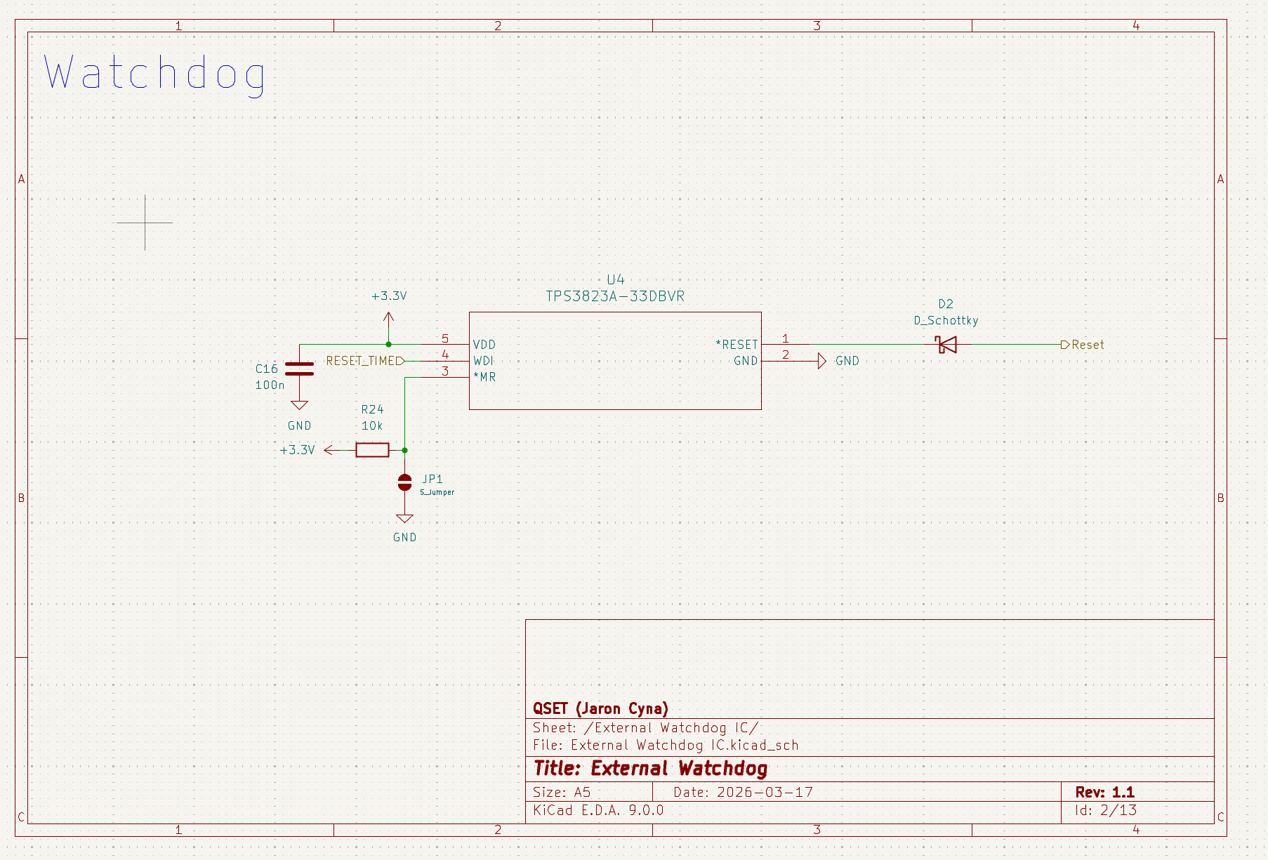
I used a Schottky pointed towards the NRST pin as it allows me to pull up the pin to 3V3 when not being used to stop accidental shutdowns, while still allowing the IC to pull it low when needed.
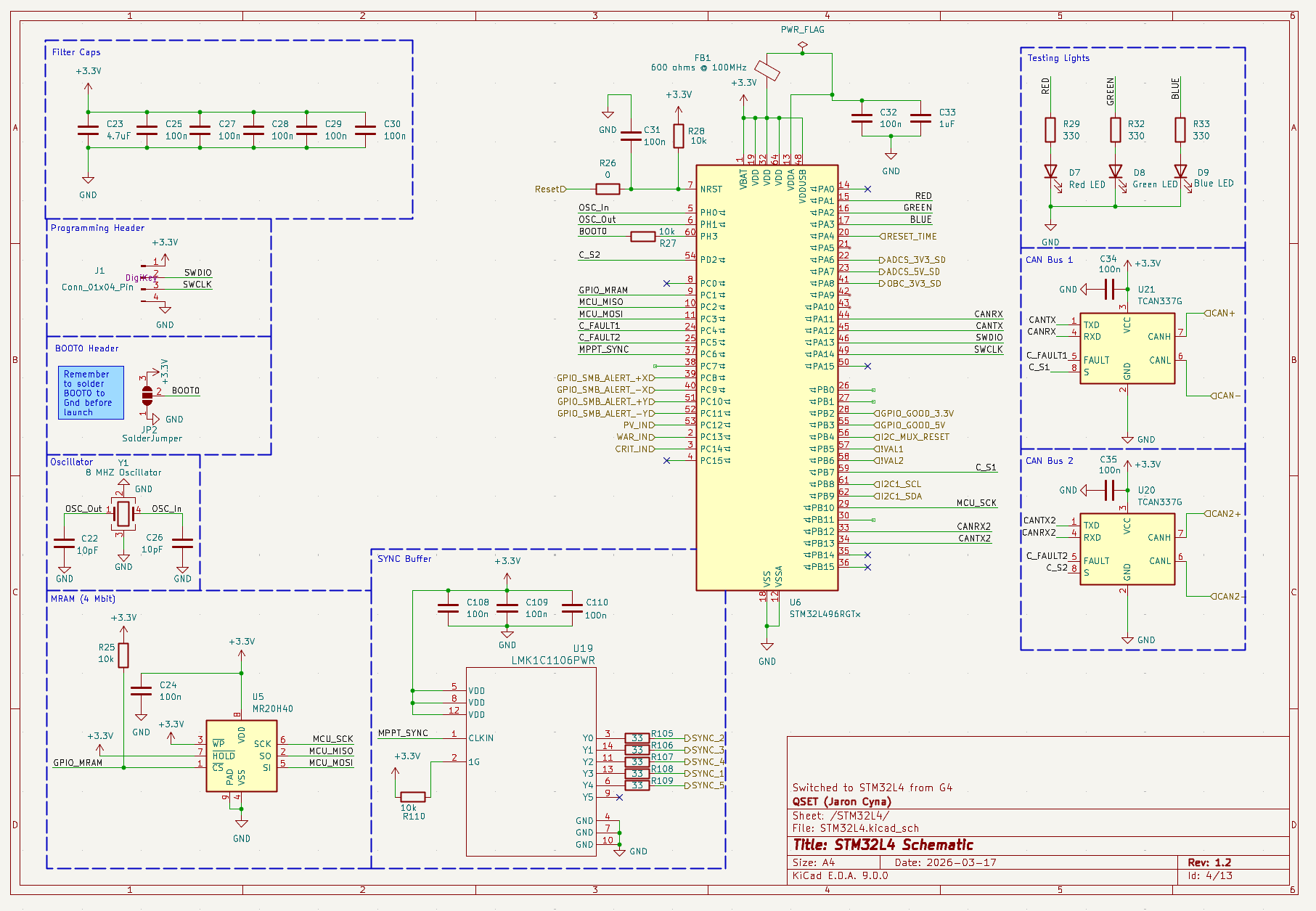
MCU Changes
Above I gave a lot of good reasons that the previous design needed the STM32G4 over the STM32L4. This primarily rested on the HRTIM, which would’ve allowed for the resolution needed for the gate driver. But now that there is no gate driver, there is no reason not to use the more efficient STM32L4. (Note I initially chose the STM32L474 but later switched to the STM32L496 for its dual CAN transceivers).
There are a few more notable design decisions here but nothing too crazy:
- MRAM: I decided to have 4 MB of MRAM since it is completely immune to SEU and TID, meaning if the MCU shut down for whatever reason, the immediate past telemetry would’ve been saved.
- Oscillator: For the oscillator I decided to use a 4 pin one (with OSC in and out along with two GNDs) since it has a much superior vibration profile to the standard 2 pin crystal oscillator.
- PWM Buffer: Another thing I added was a 1:6 PWM buffer which allows for the 1.5 MHz PWM from the MCU to be split and given to all SYNC pins on the board.
- Dual CAN: The last main change I made was adding the dual CAN transceivers which was adopted by the team based on a European CubeSat standard.
Below is the schematic for this element of the design.
Added 3V3 and 5V Buck
This was a new element to the design. Earlier in the design phase, it was hard to know exactly what logic levels the other satellite boards would need, making picking a buck harder, but now it is confirmed that 3V3 and 5V are the only levels apart from VBAT needed.
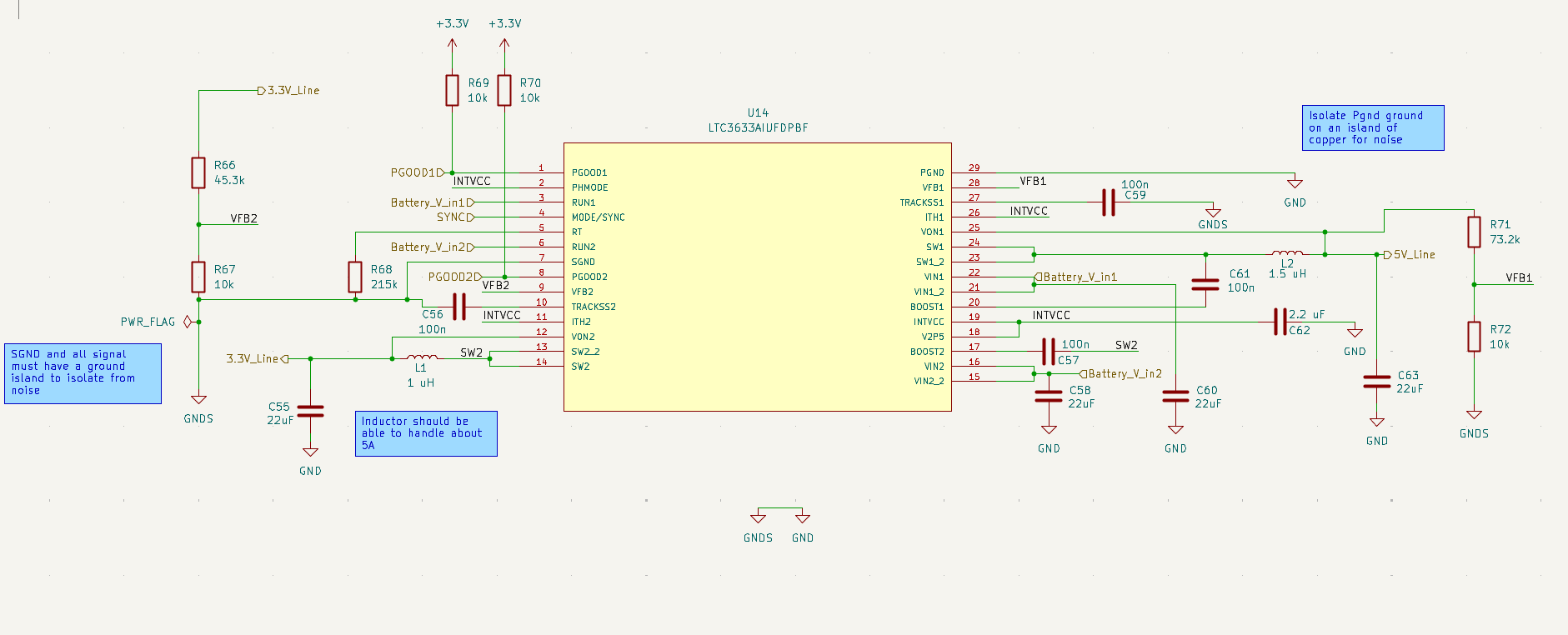
I wanted to keep all switching components on the top layer of the board to minimize EMI impact for the digital components, however, there were already 4 bucks on the board, and I needed to find 2 more which seemed unrealistic. While searching, however, I found the LTC3633 which is a dual monolithic synchronous buck converter. This made it just about the perfect IC for the needs.
Using the datasheet’s equations the inductor values were determined to be 1 µH and 1.5 µH for 3V3 and 5V respectively, with both using a 22 µF output cap. Below is a simulation of the component in LTSpice with actual ESR, ESL, and ESC parameters from the chosen components for a more realistic ripple.
Note that the Caps are simulated as 15uF due to the DC bias effect removing some capacitance from the baseline
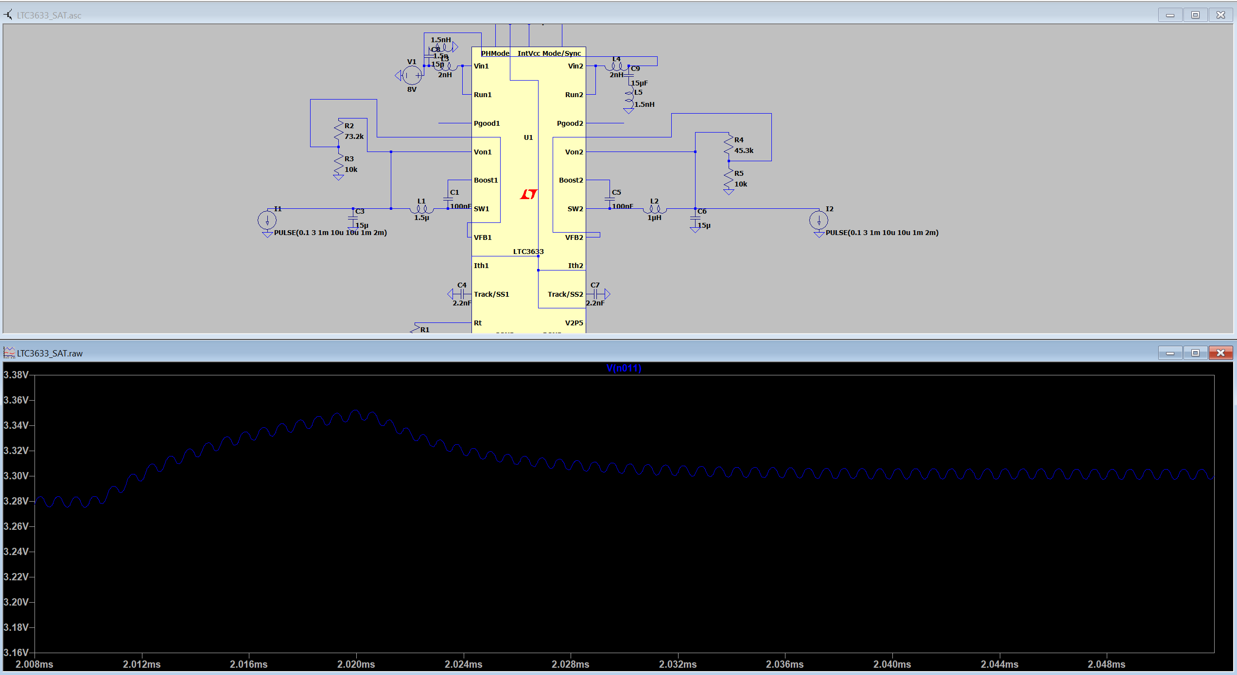
Above is a simulation of the 3V3 output of the buck converter. As you can see, the hump is a jump going from 0.1A to 3A from a current source on the output instantaneously causing a small ripple. In general though, the simulated ripple is around 10-15 mV which is quite good and allows me to avoid wasting power by using an LDO.
Here is the schematic for this circuit.
Added Sensing Circuitry
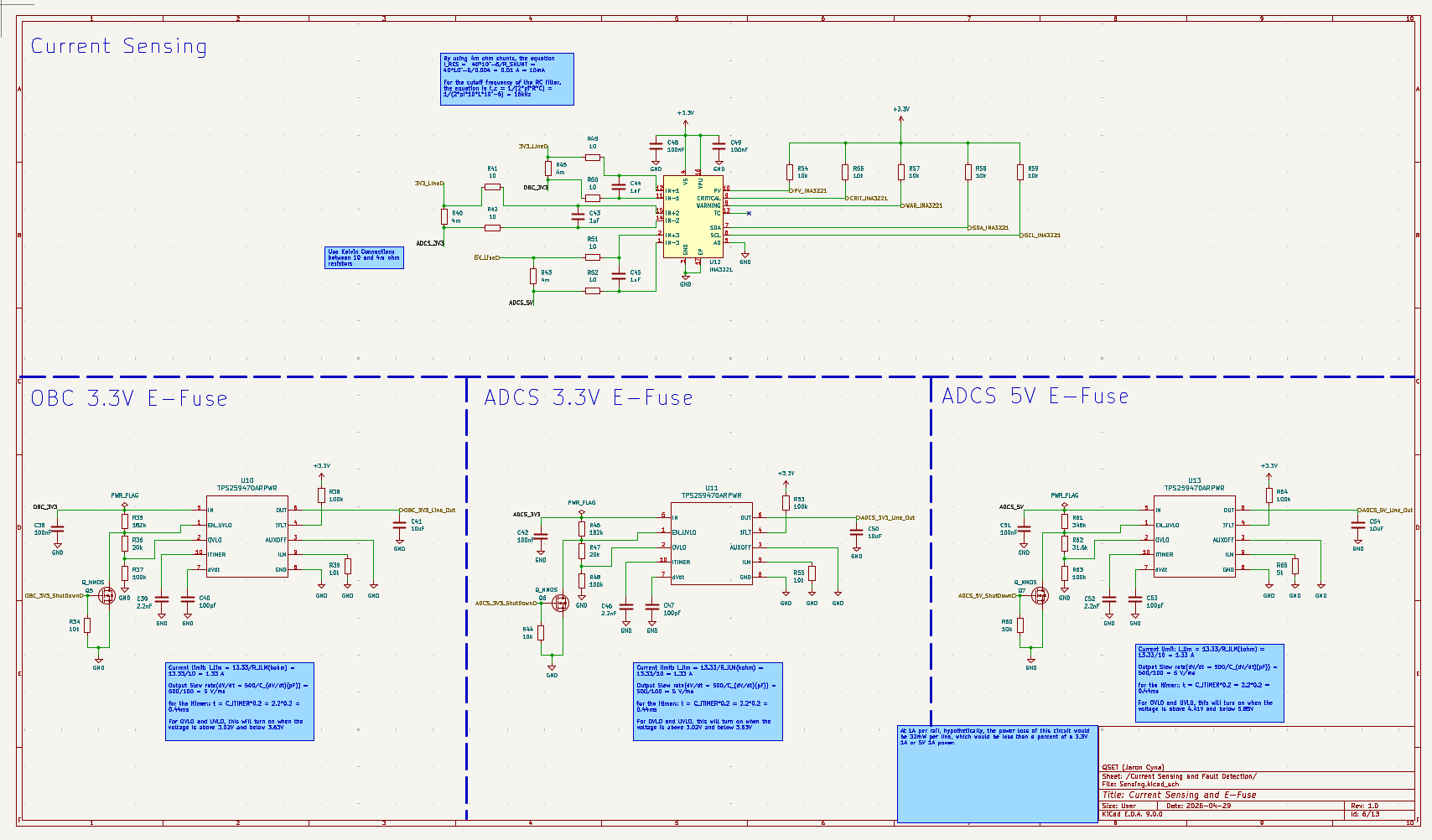
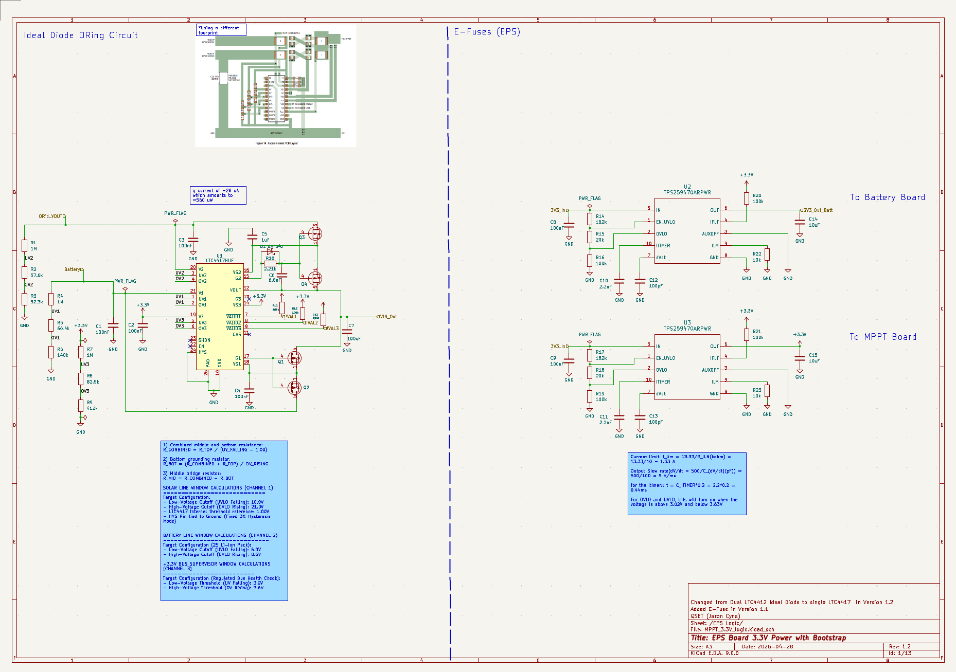
Knowing how much power is being given out is a vital part of building an EPS board. Due to this, it was decided to use an I2C current monitor (specifically the INA3221) for all output rails individually which would allow for easy calculations, along with board level shutdown mechanisms. Below are some example calculations used for the 3V3 rail’s sensing circuitry:
- Current Limit Threshold ($I_{\text{LIM}}$): Using a $10\text{ k}\Omega$ programming resistor ($R_{\text{ILIM}}$), the maximum trip current is clamped to $1.33\text{ A}$: \(I_{\text{LIM}} = \frac{13.33}{R_{\text{ILIM}}\ [\text{k}\Omega]} = \frac{13.33}{10\text{ k}\Omega} = 1.33\text{ A}\)
- Output Slew Rate & Inrush Current Control ($\frac{dV}{dt}$): To prevent voltage sagging on the upstream battery bus during hot-plugging and turn-on, a $100\text{ pF}$ capacitor controls the output rise time to $5\text{ V/ms}$: \(\frac{dV}{dt} = \frac{500}{C_{dV/dt}\ [\text{pF}]} = \frac{500}{100\text{ pF}} = 5\text{ V/ms}\)
- Overcurrent Fault Blanking Timer ($t_{\text{ITIMER}}$): With a $2.2\text{ nF}$ timing capacitor ($C_{\text{ITIMER}}$), transient current spikes are tolerated for $0.44\text{ ms}$ before triggering a fault shutdown: \(t_{\text{ITIMER}} = C_{\text{ITIMER}}\ [\text{nF}] \times 0.2 = 2.2\text{ nF} \times 0.2 = 0.44\text{ ms}\)
- Voltage Monitoring Window (UVLO / OVLO): The undervoltage and overvoltage lockout resistor dividers establish a tight operational window for the $3.3\text{V}$ rail: \(\text{Operational Window: } 3.02\text{ V} \le V_{\text{IN}} \le 3.63\text{ V}\) (Disables output below $3.02\text{ V}$ to prevent brownouts, and trips above $3.63\text{ V}$ to protect downstream ICs from overvoltage).
Each of the eFuses would then have a MOSFET attached to the EN_UVLO line which when given a signal by an MCU (either OBC or this board OR’d together via diodes) would shut down that power line. This gives flexibility for low power and failure modes. Below is the schematic page used for this telemetry and fault detection.
3V3/EPS Logic
This is another circuit that has majorly changed since the previous design. Initially I was planning on using a separate buck for the 3.3V rail for the 2 EPS boards, however, due to the added failure modes this created, I decided against it. Instead I implemented what previously only bootstrapped the EPS buck for the full buck.
However, I used a new IC, the LTC4412. This is a very interesting circuit as it mainly functions to let the battery through, however, if the battery is too high/low voltage it will fall back on the VOUT of the LTC4162 allowing for power to stay on the sat while technically dead. Additionally it has a third input which I chose to use to monitor the health of the 3V3 rail which can then be used to notify OBC that it is using its LDO from VBAT since the 3V3 line is down.
Additionally, there are 2 more eFuses (the same TPS25947 as before) which are for the 2 EPS boards. Below is the schematic for this circuit:
PC104/Connectors
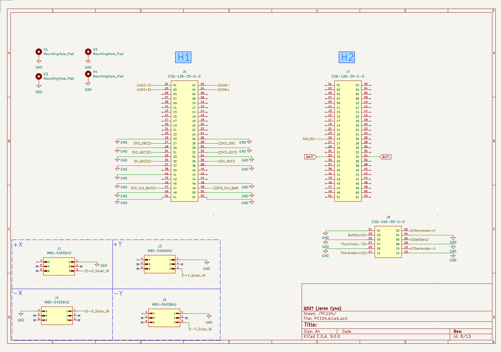
Finally, I added the connector interface which will allow this board to connect to the entire bus. This includes:
- The primary PC-104
- 4 connectors for the 4 solar boards
- An extra connector which gives the battery board direct access to the MPPT board allowing for Kelvin connections and analog thermistor inputs to avoid the noisy PC-104 interface.
Below is the schematic for this as well.
Other General Changes
There was a lot of general learning that was done while designing this board:
- Capacitor Sizing & Launch Vibrations: On CubeSats, when using ceramic capacitors, sizes over 0603 have a much higher chance of cracking during launch. Because of this, I initially wanted to use J-lead caps for all large capacitance values. However, due to parasitic inductance of the leads, they likely would’ve introduced problems in the hot loops. What I settled on instead were soft-termination caps which can survive a little more vibration than regular MLCCs.
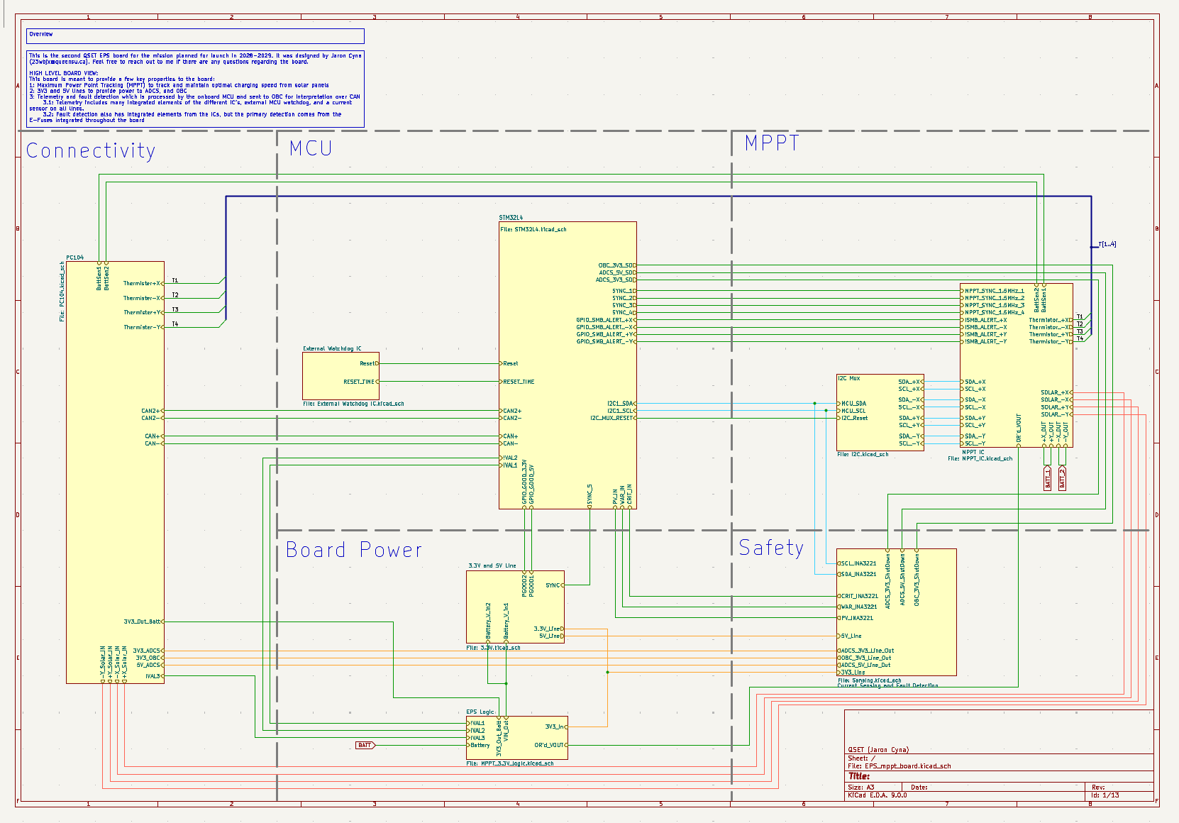
- Hierarchical Schematics: Another thing was I changed to using hierarchical labels which allowed me to make a top level sheet to help see how everything connects:
Board Layout
For the board layout, there were a few key things I kept in mind:
- First was I wanted all switching components on the top layer of the board to minimize EMI problems.
- And the second was I wanted two GND planes, also for EMI reasons.
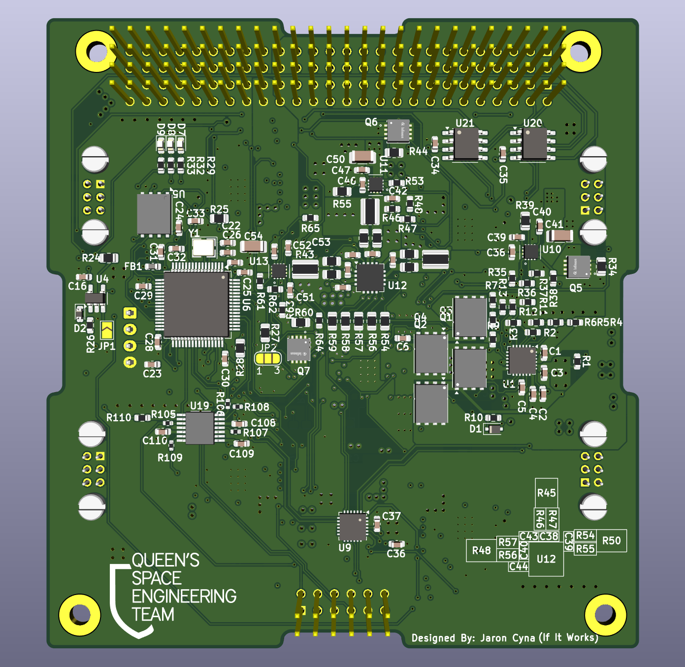
I ended up going with a 6-layer stackup consisting of: Switching, GND, Mixed (Pwr+Sig), Mixed, GND, Digital.
The 4 ports placement was chosen strategically to allow for the 4 MPPT ICs to be on opposite corners of the board so they don’t interact, leaving the centre open for the dual buck. This makes the top of the board quite cozy, while still having a fair amount of space between the hot loops.
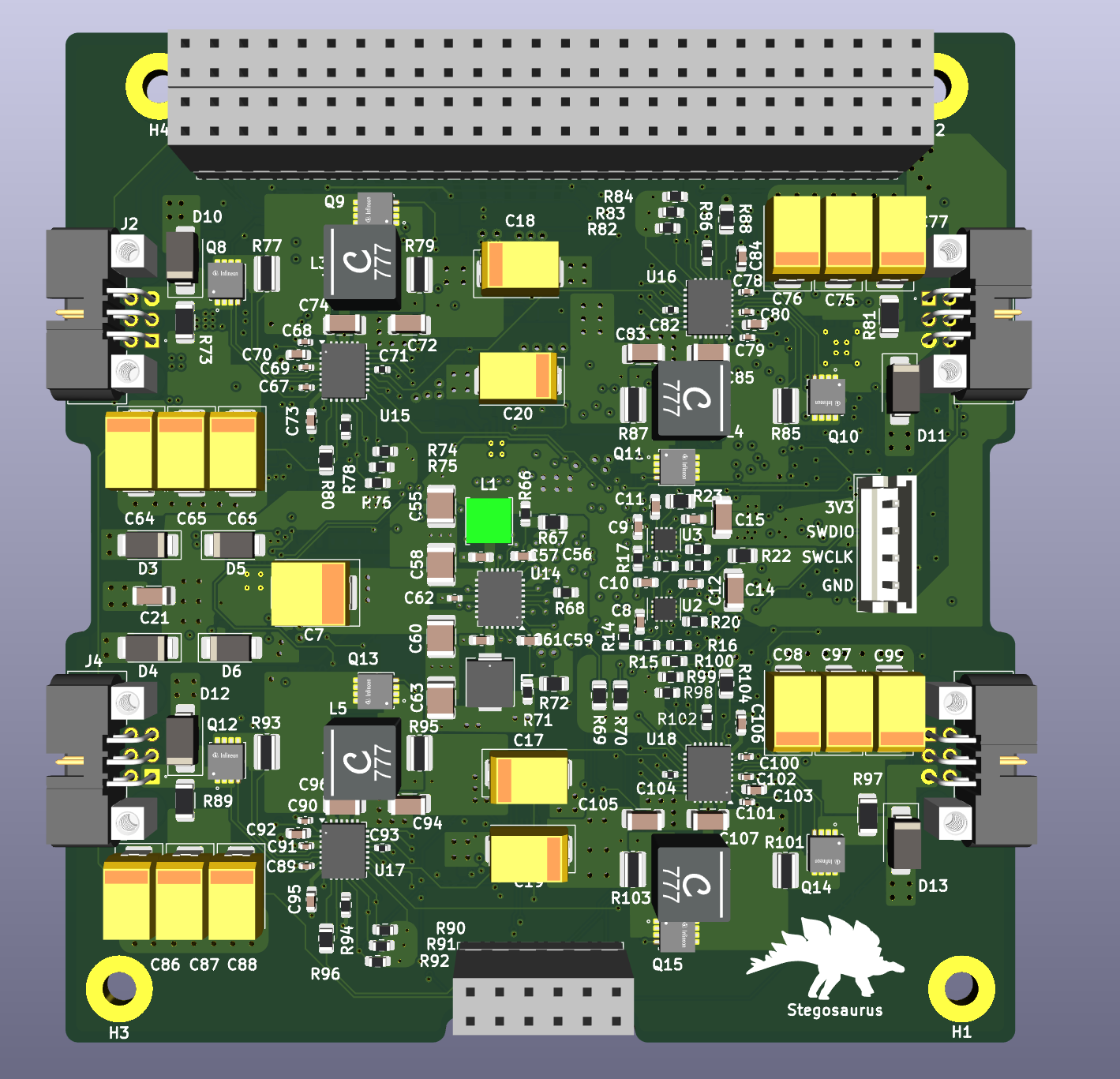
As for the bottom of the board, a lot of the components needed to be placed close for EMI or resistance reasons leading to a slightly cramped layout even with extra room. The LTC4412 fits right under the LTC3633 which allows for a few vias to take the current up in a fairly seamless way which was a satisfying thing to route. As for the MCU, it’s a little off to the side as the middle has tons of vias making it hard to route. I then turned the entire bottom unused space into a makeshift GND plane to minimize the EMI between wires.
Below is a render of the bottom of the board.
Conclusion
Overall, I’m really proud of how this board came out. I learned a lot about power electronics and PCB design, and I’m excited to see how it performs in the FlatSat in December. I learned the value of questioning your decisions and following requirements to a tee, along with the importance of really thinking through every possible failure mode.